Proper PCB Layout Minimizes Noise Coupling for Point-of-Load Converter Modules
投稿人:电子产品
2012-07-24
Modern electronic system boards require multiple non-isolated point-of-load (POL) DC/DC converter modules to power numerous ICs including microprocessors, memory, logic and other semiconductor chips. Because these multilayered printed circuit boards (PCBs) are densely populated, the POL modules used to power such devices are also highly integrated with discrete passive and active components in a miniature package.
Since these modules are switching regulators operating at high frequencies with fast transient response, they must be placed properly on the PCB with appropriate power/control routing to minimize noise coupling, ensure trouble-free operation, and maintain their optimal performance.
As noted in the Lineage Power (now GE Energy) application note AN04-006¹ entitled “Application Guidelines for Non-Isolated Converters,” switching DC/DC converters are a source of rapidly varying electrical and magnetic fields. As a result, they generate an EMI spectrum that can range from a typical switching frequency of around 300 kHz (for GE’s Austin Lynx II series modules) to harmonics in the megahertz range. Hence, to minimize the effect of these undesired frequencies on other components on the board, the location of the DC/DC converter module on the PCB is critical. The module, therefore, must be placed carefully on the board, taking into consideration the location of other components around it.
Besides employing right filtering at the input and output terminals of the modules, proper layout of the interconnects or traces connecting the power modules is also recommended to achieve optimal performance from these converter modules.
Minimizing noise
To illustrate the PCB layout guidelines for the non-isolated POL modules, let’s consider an example layout for GE Energy’s Austin Lynx II, SuperLynx II, and TLynx series buck DC/DC converters. Because the input current of a buck converter is discontinuous, the Austin Lynx II, SuperLynx II, and TLynx series converters incorporate input filter capacitors. It is important to note that the input current into the DC/DC module comes with a significant ripple component, resulting in a voltage ripple which is superimposed on the input source.
Since this high-frequency ripple voltage and current could be a potential source of noise, it must be minimized. Thus, to avoid noise coupling, the loop area for both power and signal traces to the DC/DC converter module must be minimized. Plus, both the input and output filter capacitors must be located as close as possible to the power converter module.
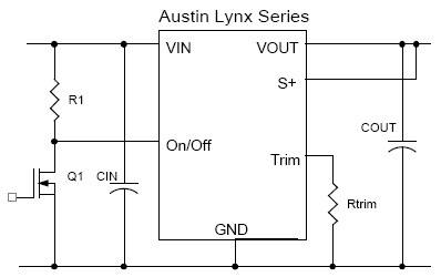
A typical application circuit using an Austin Lynx II module is shown in Figure 1. As shown, input (CIN) and output (COUT) pins use ceramic capacitors with low equivalent series inductance (ESL) and equivalent series resistance (ESR). Component manufacturers offering these capacitors, also known as bulk capacitors, include TDK and Murata. Typical value in such application is in the order of tens or hundreds of microfarads (µF).

Figure 1: A typical application circuit of an Austin Lynx II DC/DC converter module is depicted with external capacitors.
To reduce high-frequency switching noise at the input and output of the module, 0.1 μF (0603) and 1.0 μF (0603) small-package ceramic capacitors should be placed at the input and output pins of the module.
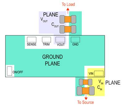
Figure 2 illustrates the physical layout for the Austin Lynx II module shown in Figure 1. This example shows important guidelines that must be followed when designing the module on a multilayered PCB. For simplicity, all three power traces (input, output, and ground) are assumed to be on the top layer of the PCB, where the Austin Lynx II module is placed.
The most important guideline here is to extend the ground plane (green color in Figure 2) to the area underneath the module. GE’s guideline does not recommended using this space for routing signal traces unless they are in inner layers underneath the ground plane. The VOUT and ground planes are placed close together to minimize interconnect inductance on the output side. Output capacitors (COUT) are connected as close to the output/ground pins as possible to provide the most effective output filtering. Similarly, on the input side, interconnect inductance is minimized by placing the VIN and ground planes close together with input capacitors placed as close to the input/ground pins as possible.

Figure 2: Simplified printed circuit board (PCB) layout for Austin Lynx II converter module.
Recommended PCB layout
In short, the Austin Lynx II DC/DC converter is so placed that it minimizes loop area and noise coupling. The signal traces should not be routed underneath the module, unless they are sandwiched between ground planes, to avoid noise coupling. Similarly, to prevent any coupling, no component should be placed under the module. As shown in Figure 2, only the ground plane is placed under the module.
For ease of repair and removal of the surface-mountable DC/DC module from the PCB, a clearance of 4.0 mm (0.16 in.) around the outline of the module is recommended. Aside from clearance, it also isolates adjacent components from exposure to heat during the removal process.
What is more, the GE guideline also recommends using copper planes for routing power traces, including the input, output, and ground connections. Traditionally, in multilayer PCBs, top and bottom layers are primarily used for routing signals. This leads to the inner layers being used for ground, input, and output. With non-isolated converter modules, since the input voltage is often used to feed multiple modules, one layer is normally assigned to it. The output can either be another layer or part of the same layer.
However, in the case of surface-mountable modules, multiple vias are needed to carry the current from the top layer to the inner power planes. The rule of thumb here is to have 3 A per via, and the recommended via size is 22 mils (0.022 in. or 560 μm) plated-through hole. For control pins, one via per pin is deemed to be sufficient. The vias also should be located in the direction of current flow for optimum performance. One or two vias per capacitor connection are recommended for bulk capacitors.
For signal traces, the company recommends a trace width of 7 to 10 mils (180 to 250 μm).
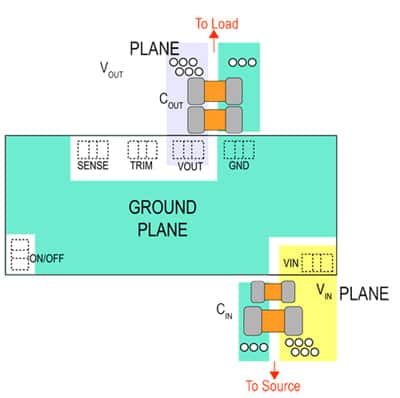
Figure 3 shows a layout of the Austin Lynx II module showing vias located near the output, input, and ground pins for carrying current to the inner layers.

Figure 3: Recommended PCB layout for Austin Lynx II converter module shows placement of vias.
Although the internal test results are not presented in the application note referenced,¹ the maker says that following the guidelines presented here will minimize noise and EMI problems associated with mounting POL DC/DC converter modules on multilayer PCBs.
Reference
- Application Note AN04-006: PWB Layout Considerations for Non-Isolated Converters; Lineage Power (Now GE Energy)
免责声明:各个作者和/或论坛参与者在本网站发表的观点、看法和意见不代表 DigiKey 的观点、看法和意见,也不代表 DigiKey 官方政策。


 中国
中国