Flexible PLC/DCS Analog Output Module Using Only Two Analog Components
投稿人:电子产品
2012-02-14
Some programmable logic controller (PLC) and distributed control system (DCS) applications require a full function, flexible, programmable analog output solution. The circuit shown in Figure 1 can accomplish this. It has only two analog components and meets most requirements for PLC and DCS applications. The AD5660-1 low power (2.8 mW @ 5 V), rail-to-rail output, 16-bit nanoDAC®, combined with the AD5750-1 industrial current/voltage output driver, provides all the typical current and voltage output ranges with 16-bit resolution and no missing codes, 0.05 percent linearity, and less than 0.1 percent output error. The circuit also contains key features for industrial applications, such as on-chip output fault detection, CRC checking to prevent packet error (PEC), and flexible power-up options, making it an ideal choice for robust industrial control systems. No external precision resistors or calibration routines are needed to maintain consistent performance in mass production, thereby making it ideal for PLC or DCS modules.
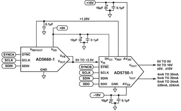
Figure 1: Basic analog output circuit for single channel (simplified schematic, all connections and protection circuits not shown).
Circuit description
The AD5750/AD5750-1 are single-channel, low cost, precision voltage/current output drivers developed to meet the requirements of industrial process control applications. The voltage output range can be programmed for the standard output ranges for PLC and DCS applications: 0 V to 5 V, 0 V to 10 V, −5 V to +5 V, and −10 V to +10 V. A 20 percent overrange setting is also provided for the standard ranges, giving the following options: 0 V to 6 V, 0 V to 12 V, −6 V to +6 V, and −12 V to +12 V.
The current output, which is provided on a separate pin, can be programmed for the ranges of 4 mA to 20 mA, 0 mA to 20 mA, −20 mA to +20 mA, 0 mA to 24 mA, and −24 mA to +24 mA. The unipolar ranges have a two percent overrange setting. Because the AD5750/AD5750-1 current output can either source or sink current, it can interface to a wide variety of sensors or actuators. The voltage and current output pins can be tied together to configure the end system as a single-channel output if desired.
The AD5660-1 is a single channel, low cost, low power, rail-to-rail voltage-buffered output, nanoDAC-integrated with an on-chip 1.25 V, 5 ppm/°C reference. The AD5660-1 incorporates a power-on reset circuit to ensure that the DAC output powers up to 0 V and remains there until a valid write command takes place.
The interface between the AD5660-1 DAC and the AD5750-1 driver is simple and requires no external components. The output voltage range of the AD5660-1 is 0 V to 2.5 V, which matches the input range of the AD5750-1. In addition, the reference output voltage of the AD5660-1 is 1.25 V, which precisely matches the reference input requirement of the AD5750-1.
Devices for PLC and DCS applications generally need ESD protection and overvoltage protection much higher than the formal recommended specifications. The AD5750-1 has integrated ESD protection diodes internal to each pin that can prevent damage from a 3 kV transient (Human Body Model). However, the industrial control environment can subject I/O circuits to much higher transients. External 30 V, 600 W transient voltage suppressors (TVS); a 50 mA, 30 V PolySwitch; and power Schottky diodes are built into the EVAL-CN0203-SDPZ circuit board to provide higher voltage ESD protection, 50 mA overcurrent, and 30 V overvoltage protection. The optional external protection circuits are not shown in the simplified schematic of Figure 1 but can be found in the detailed schematic (EVAL-CN0203-SDPZ-SCH pdf file) in the CN0203 Design Support package.
The circuit must be constructed on a multilayer PC board with a large area ground plane. Proper layout, grounding, and decoupling techniques must be used to achieve optimum performance (see Tutorial MT-031, Grounding Data Converters and Solving the Mystery of "AGND" and "DGND," and Tutorial MT-101, Decoupling Techniques).
Measurements
Integral nonlinearity (INL), differential nonlinearity (DNL), and output error are the most important specifications for PLC, DCS, and other process control systems. The AD5750-1 has highly flexible and configurable output ranges that can be tailored to meet the needs of the application. Measurements of INL, DNL, and output error for the circuit are shown in Figures 2, 3, and 4, respectively. This data was taken at 25°C in the voltage output mode using the internal current sense resistor. The AD5750-1 range was set for 0 V to 5 V. The test results for all the other ranges are listed in Table 1.
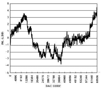
Figure 2: INL for 0 V to 5 V output range.
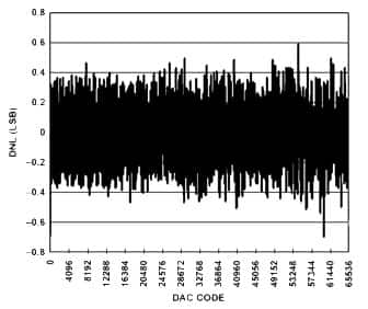
Figure 3: DNL for 0 V to 5 V output range.
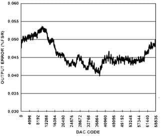
Figure 4: Output error for 0 V to 5 V output range.
The test results shown in Table 1 were made at 25°C using the EVAL-CN0203-SDPZ board powered by an Agilent E3631A DC supply and measured with an Agilent 34401A digital multimeter.
Note that the output ranges 0 mA to 20.4 mA and 0 mA to 24.5 mA are both designed to be trimmed by the customer to precisely match the 0 mA to 20 mA and 0 mA to 24 mA ranges. The 0.24 percent FSR output error measurement in the 0 mA to +24.5 mA range includes the gain error, which is removed by customer calibration.
| Range | Current Sense Resistor | INL (LSB) | Linearity (%FSR) | Output Error (%FSR) |
| 0 V to 5 V | Don't care | 7.1 | 0.011 | 0.05 |
| 0 V to 10 V | Don't care | 6.1 | 0.009 | 0.05 |
| −5 V to +5 V | Don't care | 6.2 | 0.009 | 0.04 |
| −10 V to +10 V | Don't care | 6.8 | 0.010 | 0.04 |
| 0 V to 6 V | Don't care | 6.9 | 0.010 | 0.05 |
| 0 V to 12 V | Don't care | 5.3 | 0.008 | 0.09 |
| −6 V to +6 V | Don't care | 8.0 | 0.012 | 0.06 |
| −12 V to +12 V | Don't care | 7.4 | 0.011 | 0.08 |
| −2.5 V to +2.5 V | Don't care | 5.6 | 0.008 | 0.05 |
| 4 mA to 20 mA | Internal | 6.3 | 0.010 | 0.07 |
| 4 mA to 20 mA | External | 6.2 | 0.010 | 0.07 |
| 0 mA to 20 mA | Internal | 5.8 | 0.009 | 0.06 |
| 0 mA to 20 mA | External | 5.7 | 0.009 | 0.06 |
| 0 mA to 24 mA | Internal | 5.4 | 0.008 | 0.07 |
| 0 mA to 24 mA | External | 5.5 | 0.008 | 0.06 |
| −20 mA to +20 mA | Internal | 8.8 | 0.013 | 0.05 |
| −20 mA to +20 mA | External | 9.3 | 0.014 | 0.05 |
| −24 mA to +24 mA | Internal | 9.2 | 0.014 | 0.05 |
| −24 mA to +24 mA | External | 10.1 | 0.015 | 0.04 |
| 3.92 mA to +20.4 mA | Internal | 6.7 | 0.010 | 0.03 |
| 0 mA to +20.4 mA | Internal | 7.6 | 0.012 | 0.05 |
| 0 mA to +24.5 mA | Internal | 3.4 | 0.007 | 0.24 |
Table 1: Test results for all output ranges.
Common variations
The AD5620 (12-bit) and AD5640 (14-bit) are pin-compatible with the AD5660 for applications not requiring 16-bit resolution.
For multichannel applications, the AD5623R (12-bit), AD5643R (14-bit), and AD5663R (16-bit) are dual nanoDAC devices, and the AD5624R (12-bit), AD5644R (14-bit), and AD5664R (16-bit) are quad nanoDAC devices.
The AD5751 is a unipolar analog output driver and can supply a 40 V output using a 50 V AVDD supply.
Circuit evaluation and test
Equipment needed (equivalents can be substituted)
- System Demonstration Platform (EVAL-SDP-CB1Z)
- CN-0203 Circuit Evaluation Board (EVAL-CN0203-SDPZ-1)
- CN-0203 Evaluation Software
- Software for controlling external test measurement equipment (not included on CD)
- Agilent 34401A 6.5 Digital Multimeter
- Agilent E3631A 0 V to 6 V/5 A; ±25 V/1 A Triple Output DC Power Supply
- PC (Windows® 2000 or Windows XP) with USB interface
- National Instruments GPIB to USB-B interface and cable
Load the evaluation software by placing the CN-0203 Evaluation Software disc in the CD drive of the PC. Using "My Computer," locate the drive that contains the evaluation software disc and open the Readme file. Follow the instructions contained in the Readme file for installing and using the evaluation software.
Functional block diagram
Figure 5 shows a functional block diagram of the test setup. The pdf file “EVAL-CN0203-SDPZ-SCH” contains the detailed circuit schematics for the CN-0203 evaluation board. This file is contained in the CN-0203 Design Support Package.
Setup
Connect the 120-pin connector on the EVAL-CN0203-SDPZ circuit board to the connector marked “CON A” or “CON B” on the EVAL-SDP-CB1Z evaluation (SDP) board. Use nylon hardware to secure firmly the two boards, using the holes provided at the ends of the 120-pin connectors. After successfully setting the DC output supply to +15 V, −15 V and +6 V output, turn the power supply off.
With power to the supply off, connect a +15 V power supply to the pin of CN1 marked “+15 V,” a −15 V power supply to the pin of CN1 marked “−15 V,” and “GND” to the pin of CN1 marked “GND”. Connect +6 V to CN2 the same way. Turn on the power supply and then connect the USB cable with the SDP board to the USB port on the PC. Note: Do not connect the USB cable to the mini USB connector on the SDP board before turning on the DC power supply for the EVAL-CN0203-SDPZ.
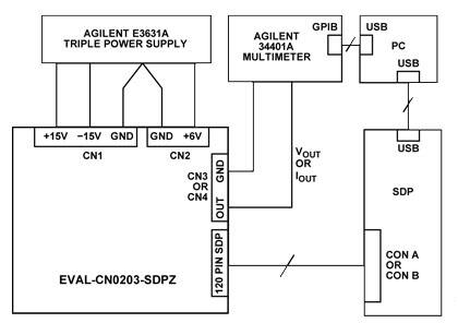
Figure 5: Test setup functional block diagram.
| Jumper | Descriptions | Setting | Function |
| JP1 | Sets the address of AD5750-1 |
Shorting Pin1 with Pin2 | Address of AD5750 : b'001 |
| Shorting Pin3 with Pin2 | Address of AD5750 : b'000 | ||
| JP2 | Sets the external compensation capacitor |
Shorting | Adding 1 nF Compensation Capacitor |
| Opening | Removing 1 nF Compensation Capacitor | ||
| JP3 | VSENSE+ Setting | Shorting | Shorting VSENSE+ with VOUT internally |
| Opening | VSENSE+ has no connection with VOUT internally | ||
| JP4 | VSENSE− Setting | Shorting | Shorting VSENSE− with GND internally |
| Opening | VSENSE− has no connection with GND internally | ||
| JP5 | Shorts the VOUT and IOUT pins |
Shorting | Shorts VOUT and IOUT together. |
| Opening | VOUT and IOUT have no connection internally | ||
| JP6 | Sets the CLEAR Mode for AD5750-1 |
Shorting | Clears to midscale |
| Opening | Clears to zero scale |
Table 2: Jumper settings for EVAL-CN0203-SDPZ (Bolded values are default settings).
Test
After setting up the test equipment, connect the pin of CN3 marked “VOUT” or the pin of CN4 marked “IOUT” to the input of the Agilent 34401A. Make sure that the cable connection on the front panel of the Agilent 34401A is correct, depending on the different input signal type (current or voltage). Testing the INL, DNL, and total error will take a considerable amount of time because all of the AD5660-1 16-bit DAC levels must be set and measured by the 34401A.
The software provided on the CD allows the DAC codes to be set by the PC. An automatic test program is necessary to step through the codes and analyze the data. This is not provided on the CD but must be implemented by the customer to correspond to the requirements of the particular multimeter used in the test setup.
In the test configuration shown in Figure 5, the GPIB output of the 34401A multimeter interfaces to a second USB port on the PC using the National Instruments GPIB to USB-B interface and cable. This allows the multimeter readings corresponding to each code to be loaded into an Excel spreadsheet in the PC. The data is then analyzed for INL, DNL, and total error using industry-standard definitions.
For more details on the definitions and how to calculate the INL, DNL, and total error from the measured data, see the "TERMINOLOGY" section of the AD5662 data sheet and the following reference: Data Conversion Handbook, "Testing Data Converters," Chapter 5, Analog Devices.
LEARN MORE
- CN-0203 Design Support Package:
www.analog.com/CN0203-DesignSupport - Slattery, Colm, Derrick Hartmann, and Li Ke, "PLC Evaluation Board Simplifies Design of Industrial Process Control Systems.” Analog Dialogue (April 2009).
- CN-0063 Circuit Note, 16-Bit Fully Isolated Voltage Output Module Using the AD5662 DAC, ADuM1401 Digital Isolator, and External Amplifiers, Analog Devices.
- CN-0064 Circuit Note, 16-Bit Fully Isolated 4 mA to 20 mA Output Module Using the AD5662 DAC, ADuM1401 Digital Isolator, and External Amplifiers, Analog Devices.
- CN-0065 Circuit Note, 16-Bit Fully Isolated Output Module Using the AD5422 Single Chip Voltage and Current Output DAC and the ADuM1401 Digital Isolator, Analog Devices.
- CN-0066 Circuit Note, Fully Isolated Input Module Based on the AD7793 24-Bit Σ-Δ ADC and the ADuM5401 Digital Isolator, Analog Devices.
- CN-0067 Circuit Note, Fully Isolated Input Module Based on the AD7793 24-Bit Σ-Δ ADC, the ADuM5401 Digital Isolator, and a High Performance In-Amp, Analog Devices.
- CN-0097 Circuit Note, Simplified 12-Bit Voltage and 4 mA-to-20 mA Output Solution Using the AD5412, Analog Devices.
- CN-0209 Circuit Note, Fully Programmable Universal Analog Front End for Process Control Applications, Analog Devices.
- MT-031 Tutorial, Grounding Data Converters and Solving the Mystery of “AGND” and “DGND”, Analog Devices.
- MT-101 Tutorial, Decoupling Techniques, Analog Devices.
- Kester, Walt. Practical Design Techniques for Sensor Signal Conditioning, Analog Devices, 1999, ISBN 0-916550-20-6
- Kester, Walt. Data Conversion Handbook, Chapter 5, Analog Devices.
- CN-0203 Circuit Evaluation Board (EVAL-CN0203-SDPZ-1)
- System Demonstration Platform (EVAL-SDP-CB1Z)
- AD5750-1 Data Sheet
- AD5750-1 Evaluation Board
- AD5660-1 Data Sheet
- AD5660-1 Evaluation Board 1
- AD5662 Data Sheet
免责声明:各个作者和/或论坛参与者在本网站发表的观点、看法和意见不代表 DigiKey 的观点、看法和意见,也不代表 DigiKey 官方政策。




 中国
中国