Protecting USB From Power Surges
投稿人:DigiKey 欧洲编辑
2013-05-28
The Universal Serial Bus (USB) has become the connection scheme of choice for interconnecting different devices, many of them providing human interface support. Support for many different types of peripheral, which can be self- or bus-powered, calls for stringent protection for not just the target device, but also the bus itself.
For example, overcurrent protection for USB-powered devices is needed, both by standards such as UL60950, as well as by the USB specification itself. Also required is good electrostatic discharge (ESD) support to ensure that devices and the host are not adversely affected by the spikes caused by plugging in devices, or the user brushing against exposed pins in the USB connector. This article looks at the requirements for protecting the power and data lines in USB and covers devices such as the TE Circuit Protection Polyswitch, the STMicroelectronics USBLC6, the Texas Instruments TPDD4EUSB30, the NXP Semiconductors IP4234CZ6, the Littelfuse 1206L family and the Bourns MF families, among others.
The design of USB peripherals poses some challenges for the engineer. The USB specification in its latest version allows for very high data rates, which puts an onus on aspects of systems design such as signal integrity. At the same time, the ability to plug and unplug devices from a live system – providing the user with an easy means to add and remove human-interface and other devices – means that the delicate electronics behind the connector need to be protected from the sudden spikes of electricity that can result from pins making or breaking contact with the host system. Designers also need to consider the effects of electrostatic discharge (ESD) caused by users touching the pins of the USB connector or cable.
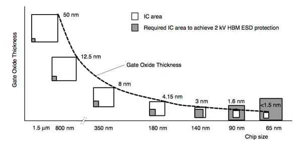
To support high data rates and overall high performance, IC vendors have moved to semiconductor processes based on finer and finer geometries. The result of the shrink in process geometry is a decrease in ESD robustness, demanding that designers implement protection measures close to the connector.
The USB specifications provide a number of options for designers to use when implementing both hosts and devices. From a power perspective, USB ports can be configured in two ways. They can be self-powered ports or bus- powered ports. This distinction affects not just motherboards and dedicated hubs. Many user-interface devices, such as keyboards, may contain low-speed USB ports to make it easier for the user to connect mice and other pointing devices to the upstream system. Devices designed for USB 3.0 cannot act as bus-powered hubs – if they provide hub services, they need to be self-powered. USB 3.0 increases the amount of energy that can be supplied to a peripheral, recognizing that the higher levels of performance supported by the latest revision of the standard are often accompanied with an increase in power consumption.
A self-powered USB hub must have the capability to source up to 500 mA on the USB power rail – Vbus – across each of its ports. A bus-powered hub can draw up to 500 mA from an upstream self-powered node. Typically 100 mA is available for the hub to perform its management functions, providing up to 100 mA per downstream port, with a maximum of four ports per hub.
As well as the USB specification itself, standards such as UL60950 demand overcurrent protection to be used in power-conversion circuitry that will supply power to downstream ports. During a hot connect or disconnect, there will often be an inrush of current from the USB hub to the USB device. This inrush can create current and voltage transients that are many times higher the operating specifications of a typical USB-connected device.
Overcurrent protection puts a limit on the amount of current that the USB device can draw from the hub or host while it is connected, in the event of a short circuit forming. This form of protection should be separate from any circuitry that limits the current demand of the USB peripheral under normal operation. It should also be designed to resist nuisance tripping, as well as voltage droops.
One form of protection is the polymeric positive temperature coefficient (PTC) device. A PTC device typically consists of a conducting polymer layer that separates two or more electrodes. When the current that passes through the device exceeds a rated limit, the polymer layer will begin to heat and turn from a solid to a liquid state, expanding as it does so. The expansion causes conductive layers within the polymer to begin to break so that the device shifts from a low resistance state to a high resistance state. As a result, current flow through the device drops dramatically. Once the fault is repaired and current flow returns to normal, the polymer cools and contracts, returning to its low-resistance state as the conducting chains come back into contact with each other.
The PTC itself provides effective protection but needs the layout to support it for best results. To ensure that the PTC is the element that trips, any current-carrying PCB traces should be designed to handle on the order of twice as much current as the PTC itself. This prevents the circuit trace from becoming the fuse element itself. Typically, on a motherboard, hub, or OTG (On the Go) device that supplies power, the PTC is placed between the power supply and the bypass capacitor rather than between the capacitor and port connector.
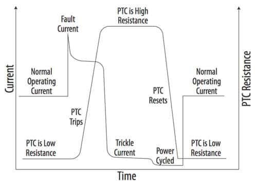
A common mistake that can lead to failures in terms of specification compliance is under-sizing of the overcurrent protection device. Sizing the overcurrent protection device with too low a current rating will add unnecessary resistance and a lower voltage. Typically, the activation current should be 2.5 to 3 times the maximum allowable port current to ensure low-enough resistance and make sure that transient currents, which can occur during power-up or reconfiguration, do not trip the protection mechanism.
As an example of what is possible in terms of transients, during initial hot-plug a compliant USB device can draw significant transient current many times above the operating power consumption. Overcurrent protection must not limit this inrush and tolerate this transient current for about 100 µs.
There are a number of PTC devices on the market, suited for use for overcurrent protection for USB applications. One example is the Polyswitch nanoSMD and miniSMD families of devices made by TE Connectivity. Devices in these ranges can handle overcurrent protection for all types of USB, up to version 3.0, and are designed to support the space constraints of many USB-based designs.
Also available are the Littelfuse range of PTCs, such as the 1206L family and the Bourns MF families of resettable fuses, which scale all the way down to 0603 sizes for extremely size-limited designs. As well as overcurrent, USB devices need to protect against overvoltage conditions. Overvoltage events can have a number of causes and need to be protected against on the power inputs of all USB-powered devices. Hot plugging is a significant cause of overvoltage events in USB devices. Testing by suppliers such as TE Connectivity has demonstrated that voltage transients caused by hot connect and disconnect, although very short, can exceed 24 V.
The difference in speeds between ports that can cope with either USB 1.1, 2.0, and 3.0 or all three provides the designer with tradeoffs to make in terms of overvoltage protection. Ports expected to cope with the comparatively low data rates of the original USB standard or the Vbus lines can afford protection devices with a higher capacitance across all lines than those used for data transfer in the USB 2.0 and 3.0 modes.
Multilayer varistors provide good overvoltage protection on power lines and lower-speed data lines in USB applications. An example of this type of device is the Littelfuse V5.5MLA0603, which is highly suited to USB-protection duties. The varistor’s resistance falls dramatically in the event of a high-voltage developing across its terminals. As a result, charge is diverted away from the power rail or signal line to ground, clamping the voltage to a much lower level, preserving downstream circuitry. Made from semiconducting ceramics, the MLA series of varistors operates over a wide temperature range and provides good overvoltage protection in a small package – often a much smaller footprint than plastic-packaged components – that resembles that of a ceramic capacitor.
The V5.5MLA0603 device is suitable for transient suppression of the Vbus and USB ground lines as it comes in a small 0603 package and supports a continuous DC voltage rating of 5.5 VDC that is consistent with the 5 V USB power supply. The V5.5MLA0603 device has a typical capacitance of 660 pF but, as the lines to be protected are for DC, the added capacitance is useful.
For high-speed data lines, Zener diodes provide a lower-capacitance solution. As overvoltage devices are often supplied with multiple protection devices within a package, it often makes sense to use Zener diodes on the Vbus power rail as well as the data lines to conserve space. The TE Connectivity PolyZen devices combine an array of Zener diodes with polymeric PTC overcurrent protection in a single package. The PolyZen devices are fully resettable and protect against multi-watt faults – the PTC element ‘trips’ to limit current through the diode under sustained faults, helping to increase the diode’s power-handling capacity. The PolyZen ZEN056V130A24LS provides effective protection for USB data lines, as it is rated for a maximum voltage of 5.75 V and a holding current of 1.3 A.
Along with overcurrent and overvoltage protection, ESD protection should be an integral part of the USB design process. Although USB transceiver ICs will have some level of built-in protection on their I/O pads, additional protection is required to maintain reliable in-field operation. Many ICs are specified to ESD levels of 1 to 4 kV as described in Mil-STD-883, Method 3015, but the tests for this standard fall short of those used by the Human Body Model (HBM) standard IEC-61000-4-2, which defines more realistic ESD scenarios for these types of product.
ESD discharge transients are very fast events, which may reach peak voltages in sub nanosecond time frames, and peak voltages and currents can reach 25 kV and 100 A, respectively. Transients of this magnitude or lower rupture the delicate gate oxides of CMOS transistors and cause other IC-level damage.
An ESD suppressor is able to react quickly, shunting the energy from the discharge to ground. The remaining energy is either dissipated within the suppressor or is reflected back towards the source of the ESD event. As with standard overvoltage protection, a TVS diode array represents one way of diverting the energy.
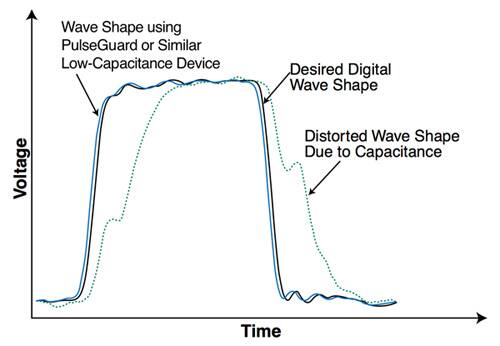
The USBLC6-2 from STMicroelectronics is designed for USB applications, protecting the two data lines and Vbus from ESD damage, supporting USB 2.0 up to 480 Mbit/s. The waveforms needed for reliable data transfer on high-speed USB 2.0 and 3.0 data lines can be distorted by any added capacitance. The capacitance of the USBLC6-2 is just 3.5 pF maximum and the device is rated to level 4 of IEC-61000. The IP4234CZ6 made by NXP Semiconductor also provides protection to IEC-61000 level 4 with a capacitance of 2 pF on each of its four rail-to-rail ESD protection diodes.
The Texas Instruments TPD4EUSB30 takes the capacitance for a TVS diode array down to just 0.05 pF, supporting the requirements of USB 3.0 and offering peak pulse current ratings to IEC61000-4-5 for protection against lightning.
The Littelfuse PulseGuard ESD suppressor uses a polymer composite material that exhibits a highly non-linear response to applied voltage. Under normal circuit operating conditions, the suppressor has a high resistance, remaining effectively transparent to the circuit. When an ESD transient develops, the suppressor resistance drops sharply. This low-resistance path redirects most of the ESD energy away from the circuit. As the applied voltage drops, the device’s resistance returns to normal. The PulseGuard suppressors present a capacitance of just 0.05 pF. Higher capacitance surge-suppression devices distort the data waveform, rounding the leading and trailing edges. The leakage current for a PulseGuard ESD suppressor is less than 1 nA, which is much less than the amount for a typical TVS diode, where leakage is often in the 0.1 to 20 µs range.
Typically, the return path for the ESD surge suppressor should be the chassis or shield ground of the system as opposed to the signal ground, preventing the discharge from coupling to the data lines and potentially corrupting transfers or having electric fields sneaking through to internal circuitry. It also means energy in the transient gets reflected back towards the ESD generator.
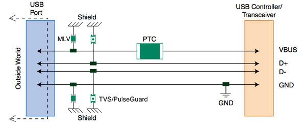
The hot-plug ability of USB brings challenges in terms of the protection measures that are needed to ensure delicate silicon devices are not damaged, but the availability of high-density devices to control overcurrent and overvoltage faults makes it possible to design robustness into a wide variety of USB devices without sacrificing space.

免责声明:各个作者和/或论坛参与者在本网站发表的观点、看法和意见不代表 DigiKey 的观点、看法和意见,也不代表 DigiKey 官方政策。





 中国
中国