


Options and Selection Criteria for 2.4 GHz Antennas
投稿人:电子产品
2012-11-29
2.4 GHz is a sweet spot for modern-day RF design can be demonstrated by mentioning a few well-known names: Bluetooth, ZigBee, Wi-Fi and WLAN. One can also toss cellular applications into the mix. Clearly, this unlicensed band allows a variety of handheld, mobile, and fixed base station designs that communicate either point-to-point, or are routed through a cellular or mesh network.
Popularity, however, brings technical issues. Even with channel segmentation, one standard’s signal can step on another and clog up throughput. Fortunately, frequency allocations, algorithms, time-slicing, and back-off timers, among other techniques, help let everyone share the band and play nicely together.
Even so, achieving optimum performance and meeting reliability goals calls for superior antenna design and close attention to the associated components that keep everything resonant. What is more, whether balanced or single ended, the transmit gain and receive sensitivity depend on the physical nature of the antenna and its radiation pattern.
This article takes a look at 2.4 GHz antennas and the coupling networks that make them work. It examines commercially available single-chip antennas that are designed to work in the 2.4 GHz ISM band. It discusses antenna types, RF distribution patterns, and range and design issues associated with using a single-chip antenna, as opposed to a connector- mounted external antenna or PCB antenna. All parts, datasheets, development kits and training modules referenced here are available on DigiKey’s website.
The signal path
Key in making your antenna perform as desired is the signal path to the antenna. While most RF chips have good output stages, matching, filtering, and splitting still may be needed, especially if a single antenna is used for more than one communications standard. As such, the typical RF output stages must still connect to either a single ended, balanced, or diplexed matching network (Figure 1).

Figure 1: While RF chips house a lot of functionality, matching to the antenna is still the engineer’s responsibility and will be different depending on the type of antenna used and if it is a shared RF stage.
Take, for example, an application that uses Bluetooth. You may have a single-ended output stage using a bandpass or lowpass filter combination to route and match the IC driver stage to the antenna (Figure 2A). A better approach is to use a balanced differential driver stage through a balun and band-pass filter (Figure 2B).

Figure 2A: A single-ended connection can take advantage of lower cost filter and matching elements.

Figure 2B: Balanced output stages used precisely matched impedance stages specific to a chip manufacturer’s part.
Fortunately, several hundred RF-Specific low-pass, band-pass, and high-pass filters as well as RF-Specific baluns and matching arrays are readily available from over half a dozen manufacturers. These can effectively block and attenuate the frequencies from cellular bands and wireless systems and pass impedance-matching, clean signals to the RF stages of the specific chip you are using.
For dense designs, a part to know about is the multi-layer Taiyo Yuden FI212C245072-T and similar parts in the series. Taiyo Yuden has found a way of updating its core technology using a multi-layer inductor to develop a 1.25 x 2 mm, combination-balanced bandpass filter and balun in a single package. Impedance values from 50 to 100 Ohms are typical, but you should note that the parts to use can be specific to a specific RF chip manufacturer.
This last item is important, as IC manufacturers will go to great lengths to characterize their RF stage and these characteristics can vary from manufacturer to manufacturer. Further, keep in mind that it is important to review the transfer characteristics of any balun and filter, especially when combined. With the Taiyo Yuden parts, frequency plots are a good way to start (Figure 3), but you will want to make your own characteristic response graphs if you deviate from the manufacturer’s suggested layout and handling.

Figure 3: Attenuation and pass-band characteristics of a combined filter and baluns can give good performance with reduced PCB footprint. In this case, a 2.4 to 2.5 GHz pass-band is created.
Both chipmakers and antenna, filter, and coupling device manufacturers are good design resources. Often, app notes and reference designs will specify the exact part number to use. To help, Taiyo Yuden offers two EMC simulators: One for waveform ¹ and one for T/Pi filters.²
The antenna
So now you have matched your RF IC stage to the antenna with good filters and baluns (if used). Now it is time to focus attention on the antenna.
For higher cost and maximum transmit power and receive sensitivity, external antenna jacks and units should be used. For high volume and cost-sensitive designs, this is typically not the way to go, especially if you can use PCB or single-chip monolithic antennas.
A PCB antenna can provide good transmit gain and receive sensitivity. Simple dipoles are easy to design and layout as a fractional or integer distance corresponding to wavelengths. As long as tight controls on the PCB manufacturing process do not let the stack up impedances vary, a reliable and repeatable design can take advantage of the PCB antenna approach.
Still, the antenna will need to be isolated from other circuitry. This takes up a good amount of space on the board where an RF ground plane and unpopulated areas are precisely located and coordinated with the mechanical enclosures and materials used in the enclosures.
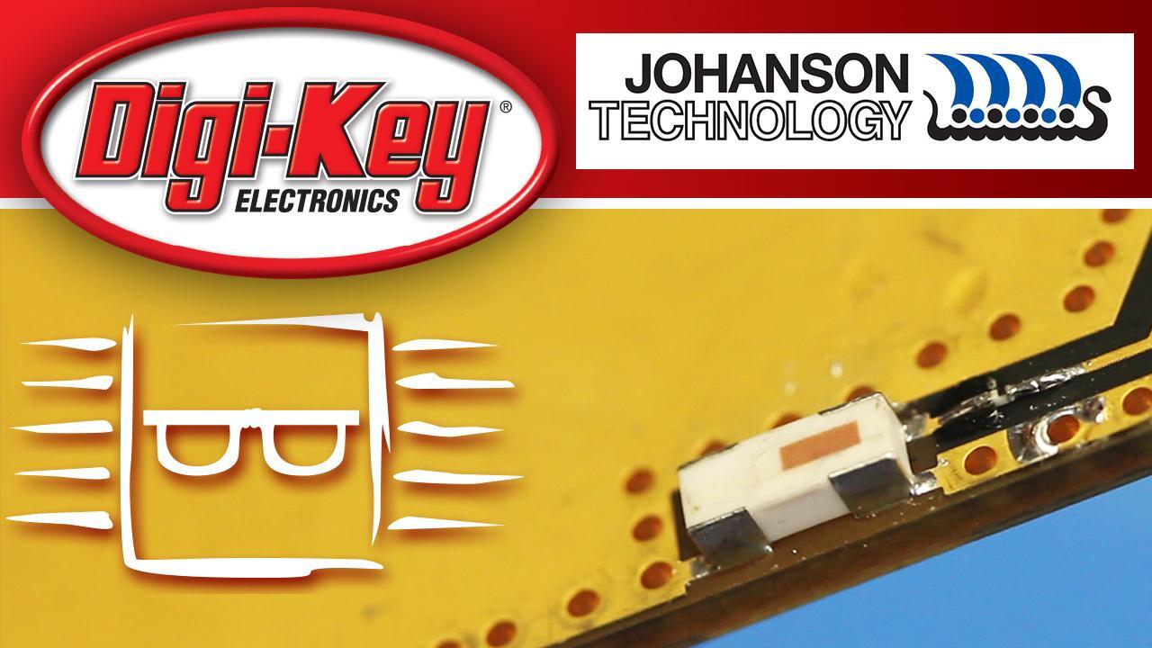
While not achieving the same performance levels as some PCB antennas, the single-chip solution allows much smaller footprints with uniform and consistent performance. Take, for example, the Johanson 2450AT18B100E passive, 50 Ohm ceramic surface-mount chip antennas. These parts use a low temperature, co-fired ceramic technology (LTCC) keeping them small for pick-and- place machines while providing near omni-directional radiation and linear polarization.
The up to 3W parts target Bluetooth, Wireless LAN, ZigBee, and WiMax applications. Specified at less than 2 for a standing wave ratio, the parts are well-centered around the 2.4 to 2.5 GHz bands (Figure 4).

Figure 4: The Johanson single-chip surface mount antennas are specified to maintain a standing wave ratio of less than two, resulting in a cleaner signal with less spurious and wasted power.
A similar single-chip antenna is the TDK ANT040015CCS2442MA1 with its center frequency of 2.442 GHz. While the max VSWR is higher than the Johanson part – at 3.5 max. TDK provides a PCB reference design with a shielded feed point that can be located remotely from the digital logic. This can help provide good range compared to when the antenna is right next to the digital logic (Figure 5).

Keep in mind that it is important to search for specifics. The TDK ANT series ranges from 2.0 x 1.25 x 0.5 mm all the way up to 9.8 x 3 x 4 mm in size. Each has its own characteristics and radiation patterns. Similarly, the Taiyo Yuden AF and AH Series contain specific part numbers on datasheets and reference materials for RF standards of interest including Bluetooth, WiMax, GPS, ZigBee, and WLAN, to name a few.
An interesting technology to be aware of is the Taiyo Yuden RadiEdge configuration where the radiation pattern is designed to emanate from the edge of a PC board. A part such as the AH316M245001-T is designated for 2.4 GHz designs and uses a 3.2 x 1.6 x .5 mm footprint with a 5 mm x 6 mm keep-out area. It may be helpful to note that the radiation pattern is also somewhat directional with around a 73 percent efficiency rating. Also, if the keep-out areas are done correctly, the RadiEdge layout can be in the middle of the printed circuit board using a two-way symmetrical pattern. This can be useful when the periphery of a PC board is tightly space constrained and may have several connectors.
Training from Taiyo Yuden and Johanson Technology is available on the DigiKey website, and provides a good introduction to the capabilities and limitations of these types of single-chip antennas and matching components.
In summary, this article has discussed design considerations and part selection criteria associated with 2.4 GHz antennas and filters. It has demonstrated how device manufacturers have stepped up to the plate to provide compact, well-designed antenna and antenna-matching solutions. Following the manufacturers’ guidelines and suggested layouts will, in the least, get your designs off to a good start.
References:
免责声明:各个作者和/或论坛参与者在本网站发表的观点、看法和意见不代表 DigiKey 的观点、看法和意见,也不代表 DigiKey 官方政策。


 中国
中国