Optimal Power Management Techniques in Energy Harvesting Designs
投稿人:电子产品
2011-11-30
Battery size constraints in energy harvesting systems necessitate creativity and innovation in order to maximize efficiency of the power source. This article will address several existing novel techniques and applications that will assist designer choices in implementing the best power solution for use in a particular energy harvesting system.
Rather than a limit on total energy, harvesting transducers impose a limit on the instantaneous power available. Since sensor networks have a physically embedded nature, they are especially well suited to exploit ambient energy sources available in certain applications.
Numerous harvesting techniques (solar, vibrational, biochemical, and motion-based) have been tried and tested. One of the challenges of harvesting energy from ambient is to convert, transfer, and store the usable power effectively. In this context, there is a need to understand and design efficient energy harvesting power management circuitry.
The typical architecture for energy harvesting power (Figure 1) consists of a power processing interface (voltage rectifier or doubler in the case of an AC signal), electrical energy storage mechanism and voltage regulation (if needed, probably using a switching regulator for efficiency).
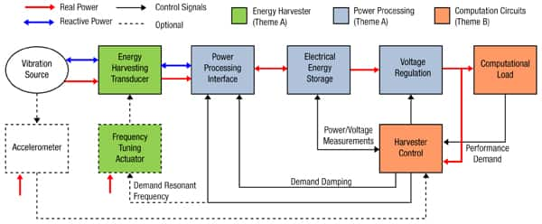
Figure 1: Power management energy harvesting circuit in blue. (Courtesy Engineering and Physical Sciences Research Council)
In this case, we are examining a variable frequency and amplitude source of energy, and for this vibration example in particular, we look at the piezoelectric transducer.
The power processing interface—AC to DC voltage rectifier
Piezoelectric sensors respond to vibration with an AC output signal (If the energy harvesting sensor has a DC output, then no rectifier will be needed and this block is simplified). Designers will most likely want to power some sort of semiconductor device which usually will require a DC voltage. Then, our first step is to rectify the AC sensor output in the piezoelectric case.
One efficient way to construct the rectifier architecture is the AC-DC doubler. Compared to a full-wave rectifier with only one large capacitor, the two half-wave rectifiers in cascade need two large capacitors, but the output DC voltage is doubled. For low vibration levels, the doubler output VS can be high enough to be used, in many cases, directly by the load without using an additional DC to DC converter. The full-wave voltage doubler is composed of a pair of series-stacked half-wave rectifiers (Fig. 2). The bottom rectifier charges C1 on the negative half cycle of input. The top rectifier charges C2 on the positive half-cycle. Each capacitor takes on a charge of 5 V (4.3 V considering diode drop). The output at node 5 is the series total of C1 + C2 or 10 V (8.6 V with diode drops).
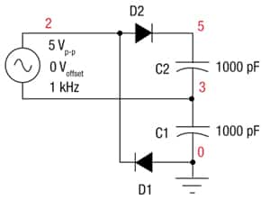
Figure 2: Full-wave voltage doubler consisting of two half-wave rectifiers operating on alternating polarities. (Courtesy of Tony R. Kuphaldt, author, “All about circuits”)
Note that the output v(5), in Figure 3 reaches full value within one cycle of the input v(2) excursion.
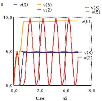
Figure 3: Full-wave voltage doubler: v(2) input, v(3)voltage at mid-point, v(5) voltage at output. (Courtesy of Tony R. Kuphaldt, “All about circuits”)
Electrical energy storage
Once the harvested sensor signal is rectified to DC, we will want to store it somehow. Replacing batteries is usually the goal, so typically a super capacitor is used for this storage role. One advantage of the super capacitor is that it has more charge and discharge cycles than a battery can supply. Other advantages of the super capacitor are high power density, high cycle efficiency, longer lifetime, and lower toxicity of material used as compared to batteries. An issue with super capacitors in energy harvesting systems is that of “cold booting.” This is a condition that occurs when the system starts running from zero stored energy. If the system starts booting up as soon as it has harvested enough energy, it is likely to drain the energy shortly after booting, forcing the system to reset and repeat the cycle of futile attempts to boot up. The better solution is to hold off booting until sufficient energy has been harvested, although being too conservative translates into increased latency. Typically comparators have been used for this function.
Cymbet has some energy harvesting evaluation boards that use their thin film EnerChip energy storage devices.
Voltage regulation—DC to DC step up or down regulator
Our next step is to stabilize the voltage with a regulator and convert it to the needed voltage to power our circuit. A regulator will also lower the ripple seen at its input. This regulator circuit must have low quiescent current and we must maximize its efficiency with the device chosen. Light load modes or discontinuous switching mode is preferable for optimum efficiency management at light loads. When light loads are sensed, the regulator enters into a discontinuous current mode (DCM), Pulse-skipping begins and quiescent current typically drops to 10s of uA. Texas Instruments’ TPS62120 is such a device for energy harvesting with integrated MOSFET’s. If a switching regulator is selected without internal MOSFET’s, then TI has the very efficient NEXFET Series, we show as an example an N-channel part CSD16406Q3 in this link.
The load circuit—computational load
Understanding the load characteristics and need for energy is critical to the eventual optimal efficiency architecture we may choose. Computational load circuits are responsible for calculating the required parameters (e.g. damping, frequency, or operating point) and sending these demand signals to the energy harvester and the power processing interface. The computational load also does the work of the wireless sensor, containing the wireless transceiver, sensors, and application software if used.
Maximizing the energy conversion efficiency with energy adaptive maximum power point tracking (EA-MPPT)
For piezoelectric materials at a given vibration status (magnitude and frequency), there exists an optimum output voltage at which maximum output power can be extracted.¹ An ultra-low-power maximum power point tracking (MPPT) scheme in a time-varying environment can be considered that tracks and holds the maximum power point periodically using a very small duty cycle, and consumes only a fraction of the power required by prior MPPT schemes. All functional blocks are activated or shut down together.
Let’s examine the typical characteristics of a solar panel (Figure 1) to explain MPPT. Isc is a short-circuit current that flows through the panel when the panel is short circuited. It is the maximum current that can be obtained from the panel.
Voc is the open-circuit voltage at the terminals of the panel. Vmp and Imp are the voltage and current values at which maximum power can be obtained from the panel. As the sunlight reduces the maximum current (Isc) which can be obtained, the maximum current from the panel also reduces.
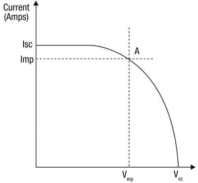
Figure 4: I-V characteristics of solar panel. (Courtesy of Texas Instruments)
Now let’s look at variation of I-V characteristics with sunlight (Figure 5). The blue curve connects the points of the maximum power at different values of insolation (a measure of solar radiation energy received on a given surface area in a given time).
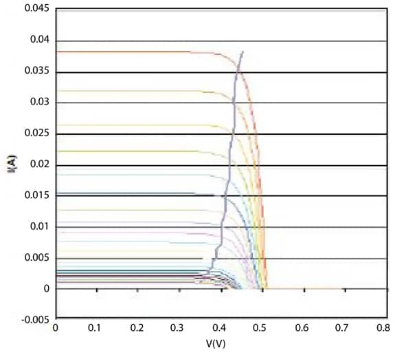
The purpose of the MPPT circuit is to maintain the operating point of the panel at the maximum power point in different sunlight conditions. As seen from Figure 5, the voltage at which maximum power is transferred does not change very much with sunlight. Using this method is the most efficient method to connect the sensor to a battery when the sensor has a DC output.
MPPT in a piezoelectric device is similarly modeled. All power, current, voltage, capacitor, and switch designations are detailed in Figure 6 for a battery-less power management unit (PMU) that manages harvested low level vibration energy from a piezoelectric device for a wireless sensor node example.¹
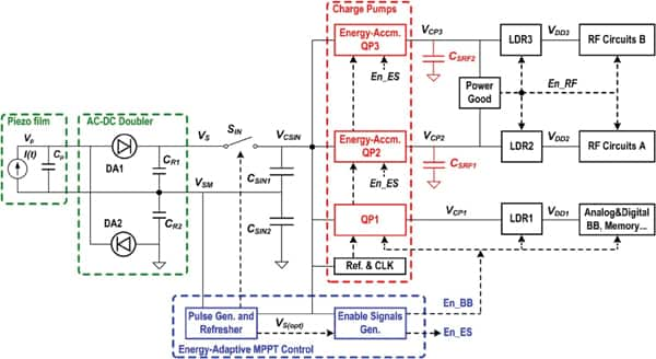
Figure 6: Piezoelectric system operational diagram. (Courtesy of Integrated Power Electronics Laboratory, The Hong Kong University of Science and Technology)
A piezoelectric film is modeled by a sinusoidal current source I(t) = Ipsin(2πft) in parallel with the internal capacitance Cp. The amplitude Ip depends upon the vibration magnitude and f is the vibration frequency. If one uses transistors as active diodes, the forward drop Vdp is close to zero, and the average rectifier output current Iinavg and the average harvested power Pinavg are:

Equation 1

Equation 2
Where VS is the output voltage of the rectifier, maximum power is obtained when VS is:

Equation 3
From Equation 2 and 3 the maximum power is:

Equation 4
To obtain the voltage VS(opt), we use the MPPT method of Equation 2, which disconnects the load by opening SIN for a very short time and senses the open-circuit peak voltage of the piezoelectric source for control:

Equation 5
It is approximately equal to the optimum voltage VS(opt) when the voltage drop Vdp is small.
The power management unit (PMU) should activate different blocks as the input power level changes. For example, at very low input power, the whole system may be duty-cycled; at medium input power the critical blocks work continuously while the rest are duty-cycled; and at high input power, all blocks are activated. To achieve energy-adaptive MPPT control, information on the absolute or relative amount of available power is needed. The problem is how to obtain and utilize this information without using power-demanding computational methods such as quantizing voltages and/or currents.
Now, here comes the energy-adaptive MPPT technique that will greatly improve the power efficiency. Since the value of VS(opt) is not adequate by itself to tell whether the available power increases or decreases, if we want to adaptively operate the individual part in different modes, a method to detect the absolute or relative amount of available power is needed.
If we use a simple “load perturbation” technique¹ and watch for level crossing events, we will be able to obtain the information of the available power level relative to the load power level.
The microcontroller
When using a microcontroller, Energy Micro has a well-suited solution for Energy Harvesting. The 32-bit EFM32 MCU is especially applicable for use in low-power and energy sensitive applications. It is a solution for applications that need to operate for as long as possible (even decades) without external power or operator intervention. Battery replacement is often not possible for reasons of access and cost.
In summary the microcontroller is characterized by very low active power consumption, reduced processing time, very fast wake-up time and ultra-low standby current. To achieve such characteristics, EFM32 has broken with microcontroller design convention in some very distinct ways. These characteristics should be in any microcontroller considered for energy harvesting:
- Very low active power consumption
- Reduced processing time
Energy Micro has built the EFM32 Gecko microcontroller around the 32-bit ARM Cortex-M3 processor core. The Cortex-M3 architecture was developed for response and power sensitive applications and is much more processing efficient than 8- and 16-bit CPUs. Tasks are therefore executed with fewer clock cycles which dramatically reduce the active period. - Very fast wake-up time
EFM32 MCUs minimize the inefficient wake-up period between deep sleep modes and active mode. This period simply cannot be neglected since low power systems continually switch between active- and sleep modes. EFM32 microcontrollers have reduced the wake-up time from deep sleep to 2 μs, ensuring as little energy as possible is used before the CPU starts processing its tasks. - Ultra-low standby current
EFM32 microcontrollers combine ultra-low power technology with clever power management to reduce energy usage in standby modes while still performing basic operations. The Deep Sleep mode includes RAM and CPU retention, Power-on Reset and Brown-out Detection safety features, and a Real Time Counter while only using 900 nA. In Shutoff mode the consumption is only 20 nA. - Autonomous peripheral operation
In addition to lowest active and sleep mode energy consumption, the EFM32 peripherals can operate in low energy modes without using the CPU. Using autonomous peripherals, an application can reduce power consumption while still performing very advanced tasks. - PRS – Peripheral Reflex System
The Peripheral Reflex System in the EFM32 microcontrollers makes it possible to directly connect one peripheral to another peripheral without involving the CPU. With this system a peripheral can produce signals which other peripherals can consume and instantly react to while the CPU remains asleep. - Well architected Energy Modes
EFM32 microcontrollers have five efficient energy modes which give system designers the flexibility to optimize their application for highest performance and longest battery life. - Energy efficient peripherals
EFM32 microcontrollers are packed with peripherals designed for low energy operation which increase the battery life 4 times compared to other low power 8-, 16-, and 32-bit solutions. Peripherals include:- LCD controller driving 4x40 segments at only 0.55 uA
- Low Energy UART, full communication at 32 kHz while consuming only 100 nA
- 12-bit ADC performing 1 million samples/sec at only 350uA
- Analog Comparator using as little as 150 nA
- Hardware accelerator for 128/256-bit AES encryption and decryption in only 54/75 cycles
- LESENSE – Low Energy Sensor Interface
LESENSE provides a configurable and energy efficient way of controlling up to 16 external analog sensors without involving the Cortex CPU. This generic low energy sensor interface works in the 900 nA Deep Sleep mode and enables autonomous monitoring of virtually any type of analog sensor control scheme, including capacitive, inductive and resistive types. For example, LESENSE can be setup to intelligently monitor sensor values and take action via the peripheral reflex system (PRS) to wake up the CPU only if programmable thresholds are exceeded – recurring, energy wasting CPU wake-ups are not necessary. - Simplicity Studio and Advanced Energy Monitoring
Cuts design cycles in half: Simplicity Studio is a free and complete tools suite providing instant and “one-click” updated access to the latest datasheets, application notes, software tools, third-party IDE, code examples, demos and other EFM32 Gecko and EFR4D Draco resources. The Simplicity Studio console auto-configures in response to user preferences, and includes access to the unique energyAware Profiler and Advanced Energy Monitoring (AEM) data for creation of energy friendly software and real time energy debugging that works in conjunction with all Energy Micro starter and development KITs.
As energy harvesting becomes a mandatory feature in ubiquitous systems, cost and size constraints will force designers to increase their design efficiency, especially in the power management portion of the circuit. By using techniques such as this article has outlined and others spurred on by new ideas from the seeds in this article, the designer will create new and more efficient architectures that will revolutionize the energy harvesting industry.
References:
- “An Energy-Adaptive MPPT Power Management Unit for Micro-Power Vibration Energy Harvesting” by Jun Yi, Feng Su, Yat-Hei Lam, Wing-Hung Ki and Chi-Ying Tsui.
- “Techniques for Maximizing Efficiency of Solar Energy Harvesting Systems”, Pai H. Chou and Sehwan Kim.
- “Harvesting Aware Power Management for Sensor Networks”, Aman Kansal, Jason Hsu, Mani Srivastava, Vijay Raghunathan.
免责声明:各个作者和/或论坛参与者在本网站发表的观点、看法和意见不代表 DigiKey 的观点、看法和意见,也不代表 DigiKey 官方政策。





 中国
中国