


Achieving High-Resolution and Zero Latency Conversion in Precision Measurement Designs
投稿人:DigiKey 北美编辑
2017-08-15
Precision control applications often present seemingly conflicting data acquisition requirements calling for both high-precision and zero-delay conversion. Developers have reconciled these requirements using complex, multi-signal-chain approaches that increase design cost and contribute to project delays.
However, it is now possible to use a single device to quickly implement high-resolution, zero-delay data acquisition designs with relatively few additional components.
This article will describe the complexities of current approaches. It will then introduce a solution that addresses these complexity and cost issues and how to go about applying them.
The complexities of high precision data acquisition
High-precision data acquisition systems typically rely on high-resolution analog-to-digital converters (ADCs) based on methods such as sigma-delta (ΣΔ) conversion. Yet, the oversampling and filtering techniques used with these methods introduce latency between the sampled event and the digital output. This latency is unacceptable for high-precision, high-speed applications. For these applications, designers have been forced into a compromise that involves creating two parallel conversion signal paths. One is based on a high-resolution ADC, and the other is based on a successive approximation register (SAR) ADC that can deliver results without delay. This compromise prohibits obtaining maximum resolution.
Using this approach, design cost and complexity increase by virtue of the additional signal chain alone. At the same time, total cost and complexity increase more subtly as designers build in compensation functions to reconcile differences in gain, bandwidth, temperature variation, long-term drift, and other performance parameters between the two signal chains.
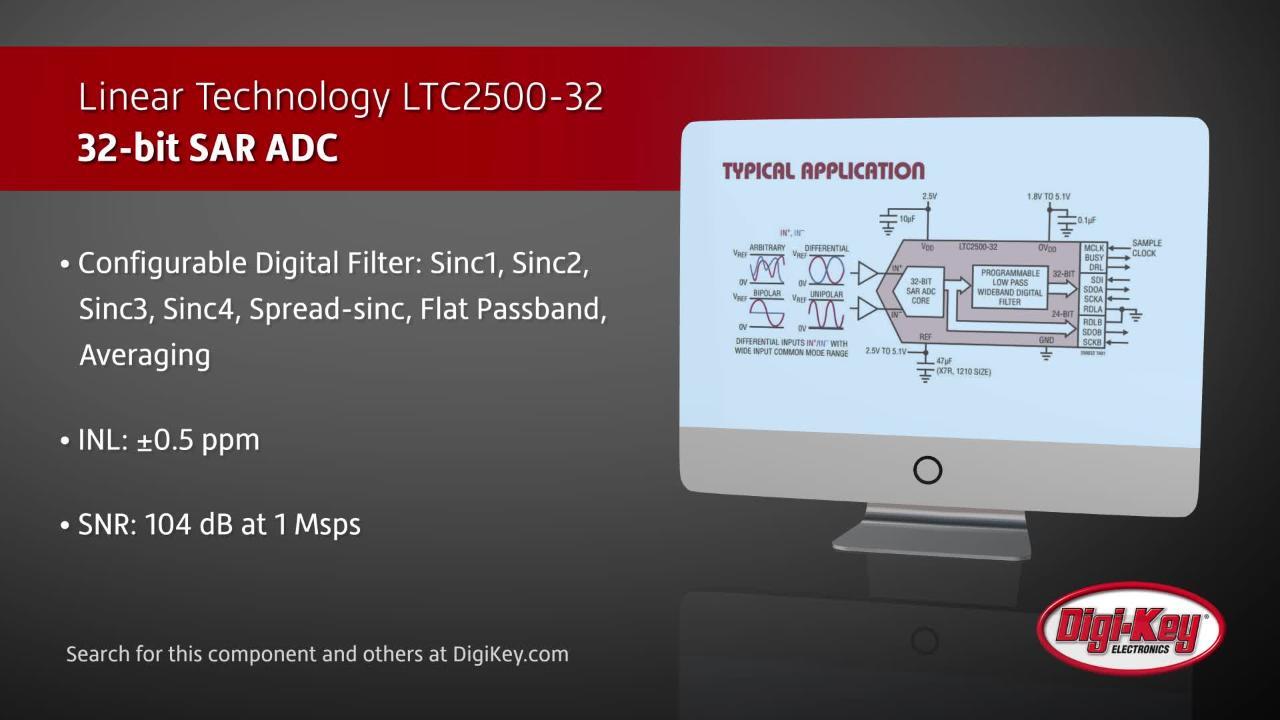
The Linear Technology LTC2500 ADC offers a simpler approach, providing both no latency 24-bit conversion and high-resolution digitally filtered 32-bit conversion.
Dual outputs
At the heart of the Linear LTC2500-32, a high-speed SAR ADC core converts analog input signals sampled from its differential analog input pins, IN+ and IN-. In turn, the output of the ADC core provides separate on-chip signal paths for the no latency 24-bit output and the digitally filtered 32-bit output from separate device pins (Figure 1).

Figure 1: The Linear Technology LTC2500-32 provides separate signal paths from a common conversion core for digitally filtered output and no latency output. (Image source: Linear Technology)
Underlying this simple view of operation, however, the device provides a sophisticated set of features that combine low-power, low-noise operation with a wide range of conversion capabilities. For example, the device helps reduce system power requirements by remaining in a low-power state while sampling its analog inputs. When the device sees a rising edge on its MCLK master clock pin, it wakes long enough to perform the conversion and automatically powers down when conversion completes. As a result, the device only consumes appreciable power during its 660 ns (max) conversion phase. This feature allows developers to optimize overall power consumption by operating the device at the lowest possible sample rate consistent with their application requirements (Figure 2).

Figure 2: The Linear Technology LTC2500-32 enters its fully active state only during its 660 ns (max) conversion phase, lowering power consumption with reduced sampling rates. (Image source: Linear Technology)
For most high-precision applications, however, the ability to deliver high-resolution data remains the dominant concern. To meet demanding conversion requirements, designers have incorporated complex filter stages on the analog input to reduce aliasing, and on the digital output to reduce out-of-band noise. For example, developers routinely condition the analog input to an ADC with a low-pass filter designed to reject signal frequency components above the Nyquist frequency – that is, half the sampling frequency.
For many applications, designers can easily meet anti-aliasing requirements with a simple low-pass analog filter. As the target signal bandwidth approaches the Nyquist frequency, however, designers need to implement more complex analog filters with sharp roll offs to eliminate aliasing without attenuating the signal itself. Using the LTC2500-32, however, developers can relax analog filter requirements by combining a simpler low-pass analog filter with the ADC’s on-chip digital bandpass filtering capabilities to create a “mixed-mode” anti-aliasing filter (Figure 3).

Figure 3: Designers can achieve a desired anti-aliasing filter (AAF) profile by combining the Linear Technology LTC2500-32 on-chip digital filter with a simple analog filter. (Image source: Linear Technology)
Digital filtering
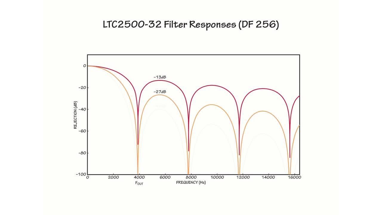
In broader terms, digital filtering meets a critical need: the removal of out-of-band frequency components that degrade overall dynamic range and conversion quality. In the past, developers often implemented complex digital filters using specialized hardware including DSPs and even FPGAs for high-speed applications. The LTC2500-32’s integrated digital filter eliminates the need for external filtering solutions, further reducing design cost and complexity. Additionally, the LTC2500-32 supports a diverse set of built-in spectral filters including a flat passband filter (Figure 4A) and multiple sinc filters (Figure 4B). Further, an averaging filter lets designers reduce the impact of random noise by averaging as many as 16,384 conversion results in the final filtered output.

Figure 4: Along with a flat passband filter (a), the Linear LTC2500-32 supports sinc1, sinc2, sinc3, sinc4 and spread-sinc (ssinc) filters (b) that developers can tune to pass or attenuate specific frequencies as needed to enhance signal acquisition. (Image source: Linear Technology)
On the output of the flat passband and sinc filters, a decimation filter down-samples the filtered data according to a programmable down-sampling factor (DF), delivering every DFth sample to the filtered output register and discarding the others. Consequently, for any ADC conversion frequency fSMPL, developers can set an effective device output data frequency f0 = fSMPL/DF when the application does not require the device’s full 1 MS/s maximum sampling rate.
The combination of these diverse filter types and sampling flexibility also enables designers to optimize the band-pass and band-reject performance of the conversion process. By configuring the device to operate at a particular fSMPL and DF, developers can move f0 for a selected digital filter as needed to pass or reject specific frequencies.
As noted earlier, digital filtering algorithms used to enhance high-resolution ADC output introduce latency between input sampling and filtered output. As filtering becomes more complex, the delay grows accordingly, regardless of the digital filter implementation method. For the LTC2500-32 ADC, the supported digital filters introduce predictable latency that grows with filter complexity (Figure 5). Within each filter type, an increase in DF adds to the effective filter length, increasing the filter’s settling time, and therefore its delay. For example, while a sinc1 filter type operating with a DF = 4 might result in a 3 microsecond (μs) delay, setting DF = 2048 would result in a 513 μs delay for the same filter.

Figure 5. Sharper roll off translates to greater latency between sampling and filtered output as illustrated here for the Linear LTC2500-32’s flat passband filter (a) and sinc filters (b). (Image source: Linear Technology)
Conversion output
Despite increased delay required for enhanced conversion results, applications that need instant conversion results can simply access the LTC2500-32 no latency output register. Following each conversion by the ADC core, the device updates the no latency output register with a 32-bit code comprising an over range detection bit, 24-bit value differential input voltage (IN+ - IN-), and 7-bit common mode input voltage (IN+ + IN-)/2. Between conversions, a host MCU can read this 32-bit register serially through the dedicated serial data output B (SDOB) pin using an associated serial data clock input B (SCKB).
Similarly, the host MCU can access the filtered data output register through a separate data output (SDOA) pin and clock (SCKA). For filtered data output, however, Linear took advantage of the extended periods between filtered output register updates associated with averaging or down-sampling. For example, when the averaging filter is set to average four samples or the spectral filter DF is set to four, the filtered output register remains unchanged during the three conversion periods prior to generation of the filtered result. With the LTC2500-32, developers can stretch the serial readout of the output register across those three conversion periods, allowing use of a slower clock for driving SCKA.
This feature, called distributed read, lets developers read a few bits of the output register between each ADC core conversion cycle. By driving the SCKA pin with at least one but fewer than 20 pulses, the host can shift out that same number of bits between conversion cycles. Developers can terminate the read process by issuing zero pulses during a conversion cycle or issuing 20 or more pulses, causing the device to update the filtered output register and initiate the next cycle of distributed reads (Figure 6).

Figure 6: With the Linear LTC2500-32 distributed read feature, developers can read out 1 to 19 bits of the filtered output register by pulsing SCKA with the corresponding number of pulses between ADC conversions (DRL low), completing the read by issuing zero pulses during the (final) ADC conversion cycle and allowing the device to initiate the next averaging sequence. (Image source: Linear Technology)
Regardless of the method used to read device output, developers need to make only a few connections to implement the digital interface between the LTC2500-32 and a host MCU. Hardware engineers can usually connect the LTC2500-32 directly to digital logic thanks to the device’s support for a digital IO supply (OVDD) separate from its own 2.5 volt power supply pin (VDD). The OVDD supply can range from 1.8 to 5 volts, enabling the device to connect directly to most digital logic components without the need for level translators.
Designers can further minimize design footprint for applications using both filtered and no latency outputs. Here, designers would connect the LTC2500-32’s separate clock and serial data lines for each output to a single clock line and a data line from the MCU (Figure 7). By toggling RDLA and RDLB, designers could separately enable the serial data output for filtered and no latency output, respectively.

Figure 7: Designers can simplify MCU interconnect by sharing clock and data connections for filtered (SCKA clock and SDOA data) and no latency (SCKB and SDOB) output, using the RDLA and RDLB to enable the respective outputs. (Image source: Linear Technology)
Designers would typically add an additional connection to connect a host GPIO to the LTC2500-32 serial data input (SDI) pin (shown in Figure 1) for programming device configuration. By setting bits in the ADC’s 12-bit control word, designers can select the filter type and down-sampling factor. During various specific operating states (such as immediately after power up or between conversions), the device opens a “transaction window” that allows the device to read in a new control word. By loading a new control word during this transaction window, they can change filter types, DF setting or other device parameters on the fly to match changes in signal characteristics or application requirements.
For most designs, however, developers would program the device just once on power-up. In some instances, developers eliminate even this device programming step by taking advantage of a pair of preset configurations built into the device. By tying the LTC2500-32’s preset (PRE) pin high, developers can choose a preset according to the state of the SDI pin. If SDI is tied low, the LTC2500-32 operates with its averaging filtering. If SDI is tied high, it uses its ssinc filter with DF=64.
Design implementation
Although the digital interface is simple, developers will typically require a few additional components to implement a practical data acquisition design. Among these external components, the selection of a suitable voltage reference is critical. The reference voltage at the LTC2500-32’s REF pin sets the maximum input range for conversion. During the conversion phase, the ADC draws charge from REF, resulting in a small current spike that could degrade conversion. Designers can largely eliminate these effects using a high-precision 5 volt voltage reference such as the Linear Technology LTC6655-5 in combination with a bypass capacitor. While the capacitor buffers the incremental current draw, the LTC6655-5 ensures that deviations of the reference voltage remain less than 0.5 ppm over the full ADC code range.
On the ADC’s IN+ and IN- inputs, designers also need to ensure that the signal remains distortion free. In theory, any low impedance signal source can be connected directly to the LTC2500-32 high-impedance input pins. In practice, however, designers would buffer the ADC’s inputs using a fast-settling amplifier such as the Linear Technology LTC6363 or LT6202 for AC applications, or a zero-drift amplifier such as the Linear LTC2057 for DC applications.
Along with buffering the inputs, these amplifiers provide the signal conditioning needed to match the input signal swing to the full dynamic range of the ADC, or convert a single-ended input to a full differential signal (Figure 8).

Figure 8: Developers can use a Linear Technology LT5400-4 resistor network and fast-settling, low-noise LTC6363 op amp to convert a single-ended bipolar AC input to a differential signal for the LTC2500-32. (Image source: Linear Technology)
The LTC2500-32’s relatively straightforward interfacing requirements allow an experienced designer to quickly implement a complete, high-resolution data acquisition design around this complex device. Regardless of design experience, however, the details of building a circuit for full evaluation of the LTC2500-32 can delay projects looking for a rapid solution. The DC2222A-A demo board simplifies prototyping and development.
The board itself provides a complete hardware implementation and associated reference design including schematics, detailed BOM, and evaluation software. On the board, a full analog input buffer circuit provides a detailed example of a signal conditioning design, backed by a detailed schematic of the multi-amp circuit. For more detailed signal analysis or application development, developers can connect the DC2222A-A demo board to Linear Technology’s Arduino-compatible DC590 or DC2026 QuikEval systems or the Linear DC890 PScope USB data collection board.
Conclusion
The growth of high-precision applications for process control and instrumentation has left developers looking for data conversion solutions able to deliver results with high resolution and zero delay. Because high-resolution conversion methods add conversion latency, developers have addressed this need by pairing a slower high-resolution ADC with a faster low-resolution ADC.
Rather than deal with the cost and complexity inherent in this approach, developers can now turn to a single device capable of delivering high-resolution with no latency output. Using the Linear LTC2500-32, they can implement sophisticated data acquisition designs capable of meeting a broad array of requirements for high-precision applications.
免责声明:各个作者和/或论坛参与者在本网站发表的观点、看法和意见不代表 DigiKey 的观点、看法和意见,也不代表 DigiKey 官方政策。


 中国
中国